

WEST LAFAYETTE — Purdue University is advancing the frontier of microelectronics through a strategic partnership with GeChi Compound Semiconductor Co. (GCCS) to accelerate the commercialization of silicon carbide. This collaboration targets the critical thermal, power, and 6G bottlenecks currently constraining the next generation of high-compute infrastructure.
The memorandum of understanding (MOU) is for five years and will strengthen collaborative research and development between both sides, as well as create academic-industry workforce development initiatives. GCCS will serve as a premier provider of semiconductor materials, and Purdue as a critical hub for the technology. It’s the first MOU between Purdue and Taiwan-based GCCS.
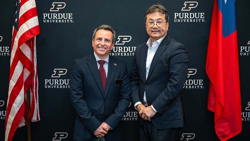
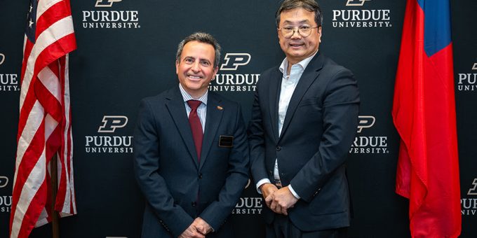
The signing was conducted on campus on Wednesday, May 27th at Hovde Hall with Dan DeLaurentis, executive vice president for research; Mark Lundstrom, chief semiconductor officer; and Zhihong Chen, the Mary Jo and Robert L. Kirk Director of the Birck Nanotechnology Center, among Purdue’s attendees. Representing GCCS were Kuo-Wei Yeh, chief technology officer; Chung-Chieh Chang, company founder; and Kuan-Ming Hsiung, board chairman.
“With this agreement, Purdue and GCCS are leveraging research strengths at the academic and industry levels,” DeLaurentis said. “It continues Purdue’s position as a leader in the latest semiconductor research.”
“This partnership represents a profound strategic alignment between GeChi Compound Semiconductor and Purdue University,” Hsiung said. “By combining our manufacturing scale with America’s leading academic institution, we are taking decisive action to secure the domestic supply chain for silicon carbide. This collaboration is not merely about advancing materials; it is about establishing the resilient, high-yield manufacturing capacity within the United States that is essential for national tech security and the future of global critical infrastructure.”
GCCS specializes in advanced silicon carbide crystal growth, bridging foundational engineering excellence from Taiwan’s premier semiconductor ecosystem with scalable manufacturing infrastructure in the United States. As AI density pushes legacy silicon to its physical limits, GCCS’s silicon carbide technology directly unlocks three critical hardware barriers:
- Thermal management: Serves as a superior wafer substrate, enabling advanced cooling via microchanneling in chip-on-wafer-on-substrate and chip-on-panel-on-substrate packaging platforms
- Power delivery: Modernizes grid-to-server power conversion with breakthrough efficiencies utilizing high-voltage direct current transmission and solid-state transformers
- 6G telecommunications: Provides the essential material efficiency required for advanced devices powering next-generation connectivity
By breaking through these physical constraints, GCCS is engineering the material backbone for the future of AI and global communications. Joint research will focus on isolating crystal defects and optimizing silicon carbide material growth to accelerate the transition to high-yield 8-inch and 12-inch wafer platforms. This collaborative framework ensures these academic breakthroughs in thermal management and material characteristics translate rapidly into high-volume commercial manufacturing.
Purdue’s national leadership in microelectronics and semiconductors is a cornerstone of Purdue Computes, a comprehensive initiative that spans computing departments, physical artificial intelligence, quantum science, and semiconductor innovation.
The West Lafayette visit by GCCS included a technical tour of the Birck Nanotechnology Center to assess key capabilities of the Purdue facility and discussions with Purdue faculty. Birck is a hub for research and houses the cutting-edge Scifres Nanofabrication Laboratory, a cleanroom, and space for interdisciplinary work. As one of the nation’s largest and most advanced academic cleanroom and characterization facilities, Birck annually serves more than 140 Purdue research groups and 25 external institutions.